[SI-LIST] Re: GND Separation for Analog & Digital circuits
- From: John Barnes <jrbarnes@xxxxxxxxx>
- To: Chris Cheng <Chris.Cheng@xxxxxxxxxxxx>, si-list@xxxxxxxxxxxxx
- Date: Thu, 26 Feb 2004 12:43:10 -0500
> ...my question remains, why does one need to create mesh power planes
> on PCB and what is the technically reason behind it. Have you yourself
> done any work to justify the methodology ?
Chris,
As an Engineer, my justification for almost all of the design techniques
that I have/do/plan to use is that they work. Since 1973, when I
started working fulltime in the computer and electronics industry:
* 9 out of 9 of the products for which I wrote the firmware at Sycor
went into production and onto the market.
* 52 out of 52 in-circuit/functional/box testers and development-
and manufacturing-support equipment that I designed at Sycor, IBM,
and Lexmark went into service--putting another 59 products into
production and onto the market.
* 47 out of 53 electronic products that I designed, or helped design,
at Sycor, IBM, and Lexmark went into production and onto the market.
* I've gotten 55 out of 56 commercial products brought to dBi for FCC
and CE Mark approval testing to pass all the relevent EMC/EMI/ESD
tests with acceptable margins--these products are, or will soon be,
in production and on the market.
To me, the major justification for meshing power and ground is cost.
For commercial products like the ones that I have developed and helped
develop for the last 31 years, saving a few dollars on the raw board
cost may make the difference between putting a profitable product on the
market, or trash-canning the whole project. For some of the products
that I worked on, coming up with a $0.05 cost savings would force an
mandatory engineering change. Adding 40% to the raw-board cost by using
a 4-layer board instead of a double-sided board, or a 6-layer board
instead of a 4-layer board, was unacceptable unless there was no other
way to complete the project on schedule.
I myself have not used the Power Mesh Architecture or the Interconnected
Mesh Power System (IMPS). But they both look like reasonable extensions
of the power/ground-gridding scheme that we have used at IBM Lexington
and Lexmark since the early 1980's on double-sided and multilayer boards
for:
* Printers.
* Typewriters.
* Multifunction printers.
* LAN adapters.
* Desktop and laptop computers.
* Keyboards, mice, trackballs, and other peripherals.
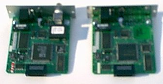
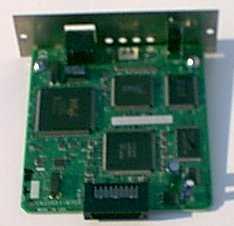
http://www.dbicorporation.com/products/etherc.jpg and
http://www.dbicorporation.com/products/etherd.jpg show two
Internal Network Adapters (INA's) that I designed and developed in the
mid-1990's, that were nearly 50% shrinks from relatively-dense External
Network Adapters (ENA's). I cut the board size from roughly 7" x 4"
down to 4.06" x 3.74", eliminating one parallel port and changing to a
higher-density parallel connector. Each of these designs took 2 spins
to go into production. These are both 4-layer boards, laid out using
what we referred to as a "submerged trace" scheme:
* Top and bottom of the board had components with traces just long
enough to via into the two inner layers--the only exceptions were
traces < 0.5" long that directly wired the ASIC to the processor.
* We encircled each IC with ground, except for the ASIC and processor
where the pair were encircled with ground.
* Otherwise, we encircled each component or clump of components with
ground.
* Wherever possible, we had ground pads under the IC's, tied to the
ground encircling the part through each ground pin of the IC, and to
the inner layers anywhere we could fit a via.
* The two inside layers had heavy power and ground grids, with ground
traces running around the perimeter of the board (ground ring).
* All signal wiring, except for the ASIC-to-processor traces mentioned
above, was run in the inner two layers. Clocks were run next to
ground traces, many of which had to be added manually. Since
plated-through holes, vias, and mounting/tooling holes were the only
things blocking these layers, we achieved very-high wiring density
even with 0.006" lines and spaces, and relatively-large vias (cheap,
cheap, cheap).
* We made a ground fence around the card, with vias spaced roughly
every 0.5" around the perimeter anywhere we weren't blocked by
connectors.
One of the peer reviewers for my book has developed double-sided cards
with up to 100MHz clocks, that meet FCC Class B and CISPR Class B
requirements without external shielding or filters. Another peer
reviewer for my book has won a number of Mentor Graphics PCB Technology
Leadership Awards for his PCB layouts. Three peer reviewers for my book
are EMC Engineers, each with two to three decades of experience in the
electronic industry. Three more peer reviewers for my book are hardware
designers and programmers with 5 to 30+ years of experience in the
electronics industry, two of whom served stints with me as Test
Engineers at IBM. The ninth peer reviewer of my book was my girlfriend
of almost 28 years, who claims that she doesn't know what I was talking
about, but sure could find my typos and grammatical errors!
Writing a technical book is the hardest work that I have ever done, and
an unlikely route to fame and fortune. For my first book, Electronic
System Design: Interference and Noise Control Techniques, which came out
in English in 1987 ( http://www.r-e-d-inc.com/english.jpg ) and
Russian in 1990 ( http://www.r-e-d-inc.com/russian.jpg ), I figure
that my net pay came to dimes/hour for all the work I put into it.
If I had continued my previous job, instead of taking a leave-of-absence
to write Robust Electronic Design Reference Book, Volumes 1 and 2, I
would have been at least $82,000 richer for 2,200 hours less work last
year--and would have had time for rest & relaxation and a social life.
But I felt that I had something important to contribute to the
engineering profession. The project definitely got out of control. I
had contracted to write a 600 page book with an August 1, 2003
deadline. I submitted the final manuscript on December 4, 2003,
totaling:
* 1,736 pages in two volumes.
* 46 chapters and 21 appendices (
http://www.wkap.nl/prod/b/1-4020-7739-4?a=2 ).
* 194 tables.
* 663 figures.
* 126 pages of indexes, with over 8,000 search terms covering about
25,000 page references.
These book(s) will be expensive, with a list price of $430 for the set.
But that is less than we charge for 3 hours of consulting or 2 hours of
EMC/EMI/ESD testing--and a tiny fraction of a company's cost and lost
profit from catching a design blunder at the very end of an electronic
development project. As a one-man EMC/EMI/ESD test house in Lexington,
Kentucky, there is a limit to the number of electronic engineers that I
can work with personally. So, in a sense I am trying to clone myself
via the book(s), to promote better electronic design practices both
inside and outside the US, and to provide the information needed to use
these design practices effectively.
John Barnes KS4GL, PE, NCE, ESDC Eng, SM IEEE
dBi Corporation
http://www.dbicorporation.com/
Cheng wrote:
>
> It all sounds great to promote your book and your service. But my question
> remains, why does one need to create mesh power planes on PCB and what is
> the technically reason behind it. Have you yourself done any work to justify
> the methodology ? I read your response and 99% of it seems to be a book and
> service promotion coupled with a pile of MCM reference paper that has
> nothing to do with PCB design. In am interest in your personal technical
> answer. Did I miss anything ?
>
> -----Original Message-----
> From: John Barnes [mailto:jrbarnes@xxxxxxxxx]
> Sent: Wednesday, February 25, 2004 2:10 PM
> To: Chris Cheng; si-list@xxxxxxxxxxxxx
> Subject: Re: [SI-LIST] Re: GND Separation for Analog & Digital circuits
>
> > What do all these MCM papers promoting mesh power distribution to do
> > with PCB power distribution design ? There are many reasons why MCM
> > or ultra fine pitch substrates use meshed power/gnd planes. They vary
> > from degassing requirements on organic substrate to via and
> > interconnect constrain like IBM TCM. However, they are fundamentally
> > different to regular PCBs. I have design many MCM and fine pitch
> > packages and I have never seen a mesh design out perform electrically
> > over a conventional solid reference planes PCB. The practice came out
> > from process requirement more than performance enhancement. I don't
> > see why it should be promoted in places where it is not necessary.
>
> Chris,
> Peter's initial posting said that he was looking for additional
> information on Power Mesh Architecture. I tried to oblige. The 9
> papers that I cited represent less than 1.3% of the reference documents
> that I have in my file on designing power distribution for electronic
> products and equipment.
>
> To me, power distribution on a chip, package, printed circuit board,
> subsystem, system, and installation are all part of a continuum.
> Strategies, techniques, ideas, and analyses that are commonly used on
> printed circuit boards may also work at the module-packaging level, or
> at the subassembly/system level, with a little tweaking to meet the
> particular situation--and vice versa. I consider the utility of ideas
> based on their own merits, not on what they are called, how they are
> currently used, who came up with them, or where I happen to find them.
>
> I am continuously searching for viewpoints, strategies, techniques, and
> ideas that can help me on current and future projects--and since I
> consider my job function as an Engineer is to "make things work"--that
> covers a lot of territory... On the average, 95% of the 300 books and
> 900 magazines/journals that I read cover-to-cover per year are technical
> in nature. I currently have 16 bookcases of electronic books, 8
> bookcases of databooks, and 6 bookcases of electronic magazines/journals
> in my personal collection, along with 20+ piles of electronics magazines
> that I've read, but haven't gotten around to sorting and putting away
> just yet.
>
> Chapter 28 "Bypassing, Decoupling, and Power Distribution" in my new
> book(s), Robust Electronic Design Reference Book, Volume 1 and 2 (to be
> available in late March http://www.wkap.nl/prod/b/1-4020-7739-4 ) is
> 42 pages long and is based on 480 reference documents that I had
> collected on the subject as of mid-November last year.
>
> Already this year, two products that clients brought to dBi for FCC and
> CE Mark EMC/EMI/ESD testing and approvals had power distribution
> problems. Both problems took us longer to find and fix than I thought
> they should. With my latest book(s) out of the way (see above), which
> chewed up some 4,200 hours of my time last year, I'm digging even deeper
> into the subject. So far I have:
> * Searched for the titles of all the papers written by 480
> authors, who were listed as the author/co-author of at least one
> book/report/paper/article/application note on the subject.
> * Gone though every issue I can find of 8 electronic engineering
> magazines/journals.
> * Gone through the every proceeding I can find for 5 electronic
> engineering symposiums/conferences.
> * Searched 34 web sites for pertinent application notes.
>
> I still need to read through about 12 inches of 2003/early 2004 EDN and
> Electronic Design magazines, and search another 44 web sites that have
> had at least one web page or .pdf file on bypassing, decoupling, and
> power distribution. Only then will I consider my search complete, and
> my bibliography ( http://www.dbicorporation.com/pwr-bib.htm ) brought
> up to date again--at least for awhile. Of the 220+ additional
> references that I have found and bookmarked/photocopied/printed out
> since late January, so far I've only found three ideas that aren't in
> Chapter 28 of my book. And none of them would help me crack my clients'
> problems any quicker. But I keep hoping...
>
> John Barnes KS4GL, PE, NCE, ESDC Eng, SM IEEE
> dBi Corporation
> http://www.dbicorporation.com/
------------------------------------------------------------------
To unsubscribe from si-list:
si-list-request@xxxxxxxxxxxxx with 'unsubscribe' in the Subject field
or to administer your membership from a web page, go to:
//www.freelists.org/webpage/si-list
For help:
si-list-request@xxxxxxxxxxxxx with 'help' in the Subject field
List technical documents are available at:
http://www.si-list.org
List archives are viewable at:
//www.freelists.org/archives/si-list
or at our remote archives:
http://groups.yahoo.com/group/si-list/messages
Old (prior to June 6, 2001) list archives are viewable at:
http://www.qsl.net/wb6tpu
Other related posts: